30+ fpga block diagram explanation
The basic block diagram is as follows. The address register output feeds back to its input using a multiplexer.
Embedded Fpga Under The Hood Electronic Design
Intel Agilex FPGA and SoC Block Diagram 15.
. Carefully programmed to account for all the various delays internal to the FPGA chip and you see these in the simulations. In order to give you a good idea about the circuit we are implementing on our FPGA lets dive into the block diagram. What you need to know.
IspLEVER Tutorials Introduction FPGA Block Modular Design Tutorial 2 Establish location and timing objectives for the top-level design. This paper presents the design and implementation of such an. FPGA Logic block diagram classic by André Daniel Christensen.
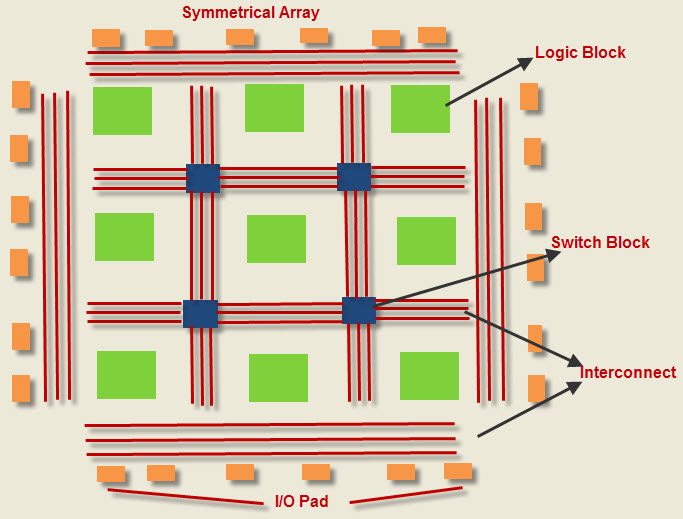
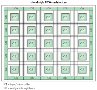
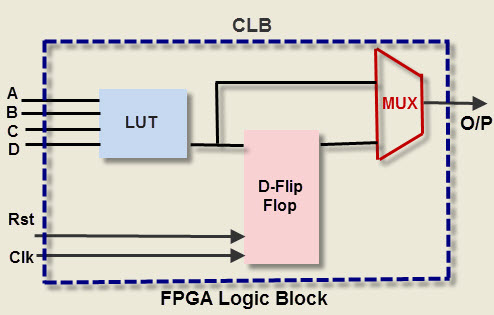
Block Definition Diagrams are based on UML class diagrams and include restrictions and extensions as defined by SysML. The irst thing we must do is create the block diagram for our project - assuming you are starting from scratch. A CLB is the fundamental component of an FPGA allowing the user to implement virtually any logical functionality within the chip.
The first static memory based FPGA called SRAM is used for configuring both logic and interconnection using a stream of configuration bits. Block diagram of the FPGA operations. 1 The programmable attribute of FPGA makes it feasible for connecting FPGA directly to various image sam-pling devices.
Todays modern EPGA contains. This is achieved by the usage of two sets of. The register output is slightly delayed with respect to the clock and.
Field programmable gate arrays FPGAs are in use to build high performance image processing systems. Field Programmable Gate Array FPGA is an integrated circuit that consists of internal hardware blocks with user-programmable interconnects to customize operation for a specific. With NDK you can easily create own FPGA-based network application for up.
Our FPGA team in CESNET Liberouter department released the Network Development Kit NDK as open-source. This FPGA has 20480 slices almost 41000 logic cells each constituted by one 16x1 LUT Look Up. They are generally used to display systems of blocks or show.
FPGA-based Digital Control Box for Phase Stabilization of a Frequency Comb. Figure 32 shows an address clock enable block diagram. Intel Agilex FPGA and SoC Family Variants 12.
XC3S2000 FPGA from Xilinx 14 has been used to implement the whole system see fig. Generate block diagram OK now the walkthrough. In contrast the GPU accelerator requires PCIe to communicate with.
Use Createlys easy online diagram editor to edit this diagram collaborate with others and export. Intel Agilex FPGA and SoC Summary of Features 14. The multiplexer output is selected by the address clock.
Archive and deploy sub-module projects.
Know About Fpga Architecture And Thier Applications
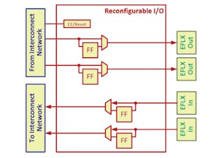
Embedded Fpga Under The Hood Electronic Design
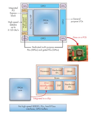
Embedded Fpga Under The Hood Electronic Design
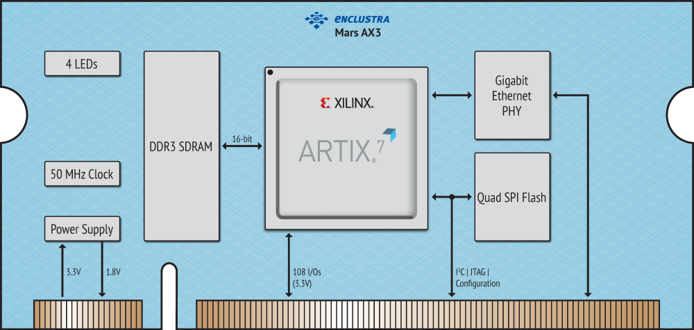
Enclustra Fpga Solutions Mars Ax3 Xilinx Artix 7 28nm Fpga Module 7a35t 7a50t 7a100t
Know About Fpga Architecture And Thier Applications

Multi Resource Scheduling For Fpga Systems Sciencedirect
Know About Fpga Architecture And Thier Applications
Embedded Fpga Under The Hood Electronic Design

Multi Resource Scheduling For Fpga Systems Sciencedirect
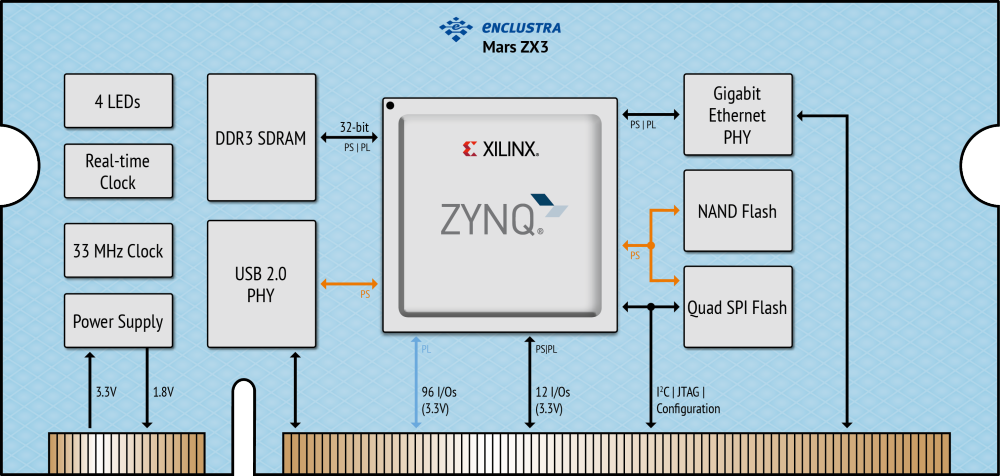
Enclustra Fpga Solutions Mars Zx3 Xiliny Zynq 7020 All Programmable System On Chip Soc Module System On Module Som Xc7z020

Enclustra Fpga Solutions Mercury Kx1 Xilinx Kintex 7 Fpga Module Xc7k160t Xc7k325t
Know About Fpga Architecture And Thier Applications
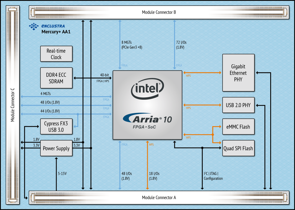
Enclustra Fpga Solutions Mercury Aa1 Intel Arria 10 System On Chip Soc Module System On Module Som 10as027e4 10as027e2 10as048e2 10as048e3
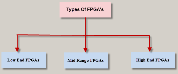
Know About Fpga Architecture And Thier Applications
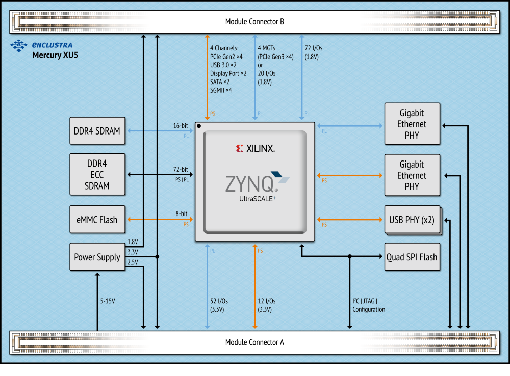
Enclustra Fpga Solutions Mercury Xu5 Xilinx Zynq Ultrascale Mpsoc Module System On Chip Soc Module System On Module Som Zu4cg Zu5ev Zu7ev Zu7evzu2cg Zu2eg Zu3eg Zu4cg Zu4ev Zu5ev
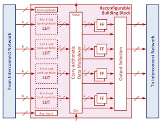
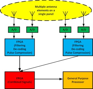
Reap The Processing Power Of Fpga Integrated Sdrs Electronic Design

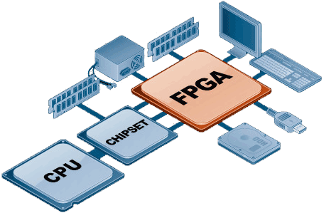
Fpgas Fpga Cpu News